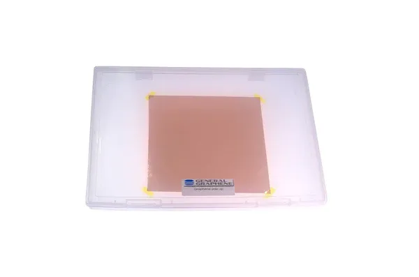
CVD Graphene Films with PMMA Coating
General Graphene
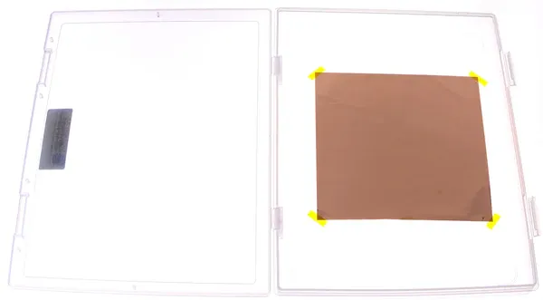
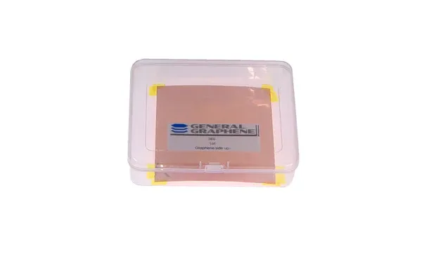
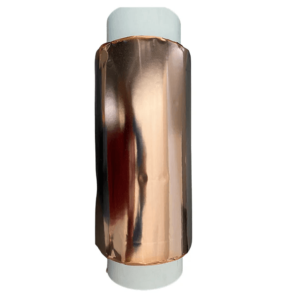
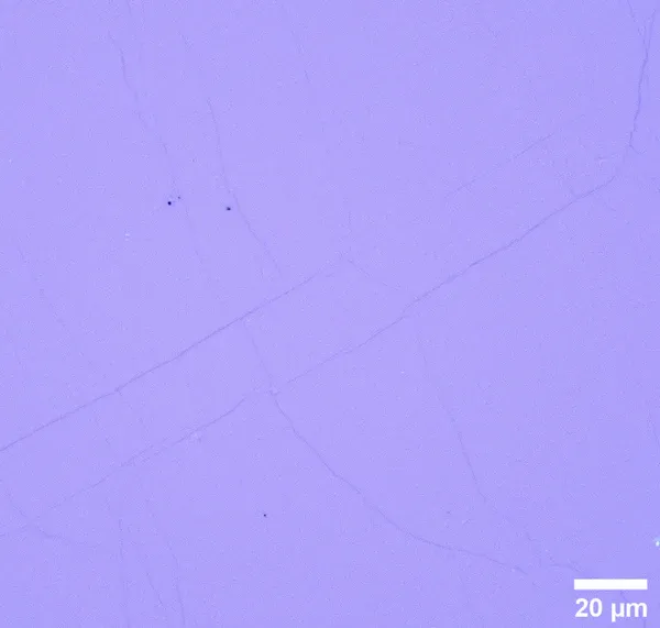
The CVD graphene films consist of monolayer graphene grown on copper foil substrates. Monolayer graphene is a one-atom-thick sheet of carbon with a honeycomb crystal lattice structure, measuring 0.34 nm in thickness. As part of the unique family of two-dimensional materials, graphene exhibits outstanding electrical and thermal properties, along with exceptional selective permeability, making it suitable for a broad range of applications.
The company offers monolayer graphene on copper foil in four standard formats, with the capability to support roll-to-roll growth and custom sizes. It also provides expertise in transferring monolayer CVD graphene onto polymers, silicon wafers, and other custom substrates.
It is also possible for the company to produce stacked bilayer and trilayer graphene on copper through a wet transfer process, available in 5 x 5 cm and 8 x 8 cm sheet sizes.
Substrate/Film type
Planar film
Coating
Graphene
Growth substrate
Predominantly Cu(111)
Sheet Resistance
500 +- 70 Ω/sq
Film Thickness
3.45 Åm
Transparency
~97.7%
Average Graphene Grain Size (µm)
~80
Multilayer Coverage (%)
< 5%
I2D/IG Average - after transfer
> 1.6
ID/IG Average - after transfer
< 0.05
2D peak FWHM (cm-1) - after transfer
~ 35
Mobility (cm2/Vs)* (dep on transfer)
> 3000
Cu Catalyst Thickness (µm)
20
Average Crystal Size (catalyst)
cm-scale
Growth Method
Chemical Vapor Deposition (CVD)
Size
5x5 cm, 8x8 cm, 15x15 cm, 20x28 cm
0 global ratings
Verified Identity
Every review undergoes an email verification process to ensure it originates from a verified industry professional.
Verified Purchase
We manually validate "Verified Purchase" claims by cross-referencing with supplier records or identifying the equipment in peer-reviewed scientific publications.
Transparent Publishing
All verified reviews, whether positive or negative, are published without bias as long as they comply with our community guidelines.
No reviews yet. Be the first to share your thoughts!
Share your experience with this product.
Scientific publications where researchers have utilized this equipment.Are you an author? Contact us to add your research.