
CVD Graphene (Chemical Vapor Deposited)
CVD Graphene Films
Price: from 90.00 USD
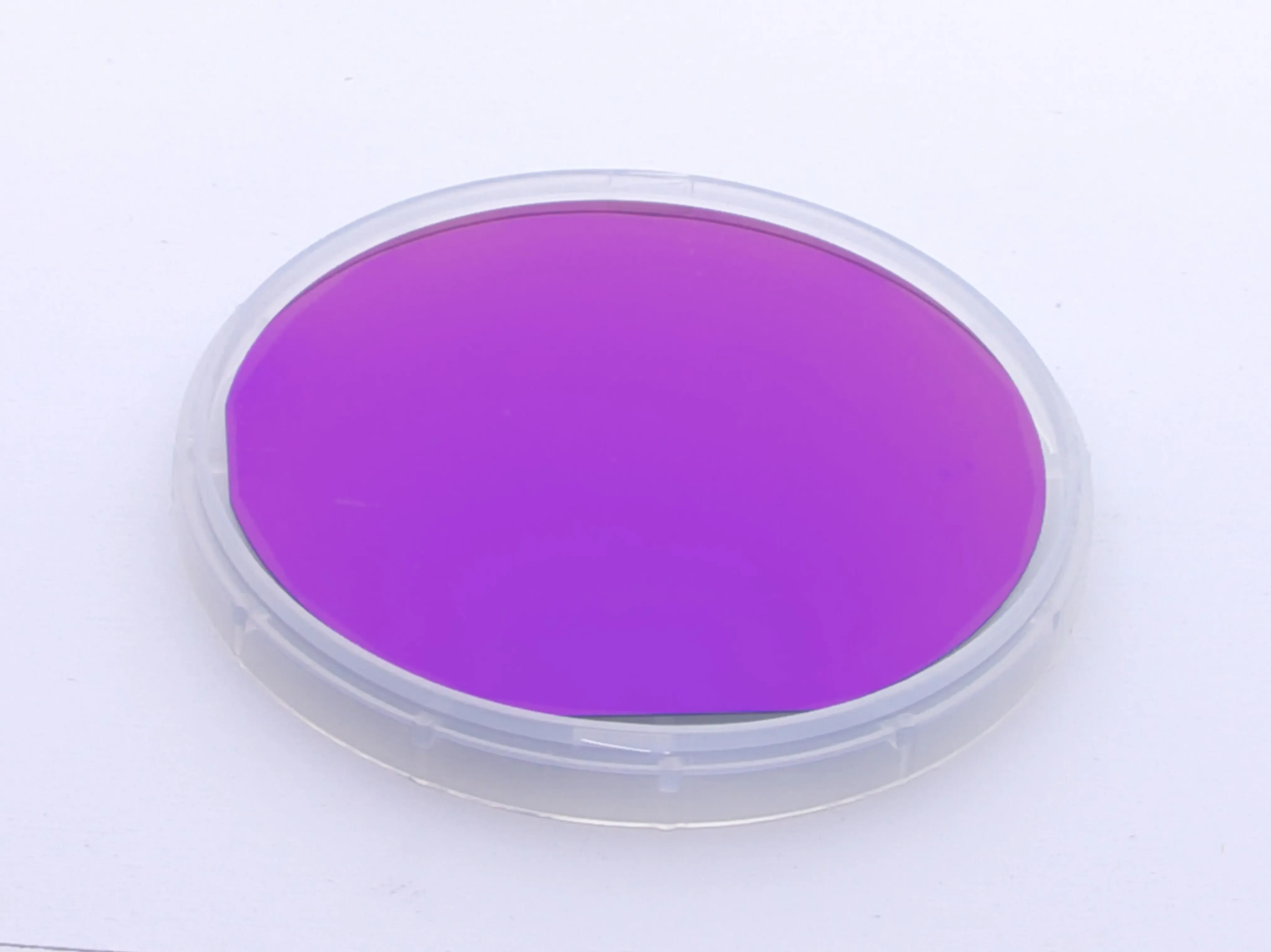
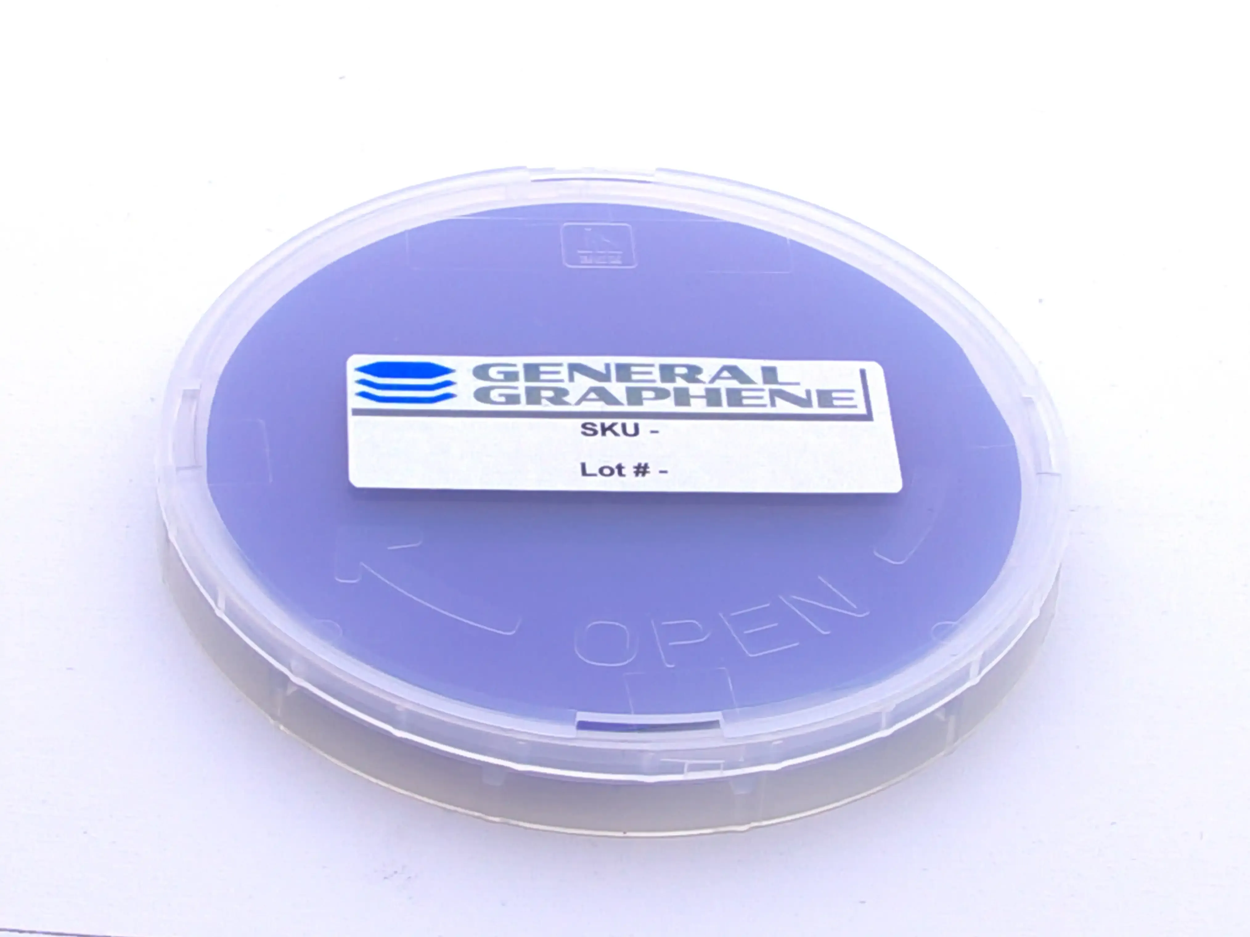
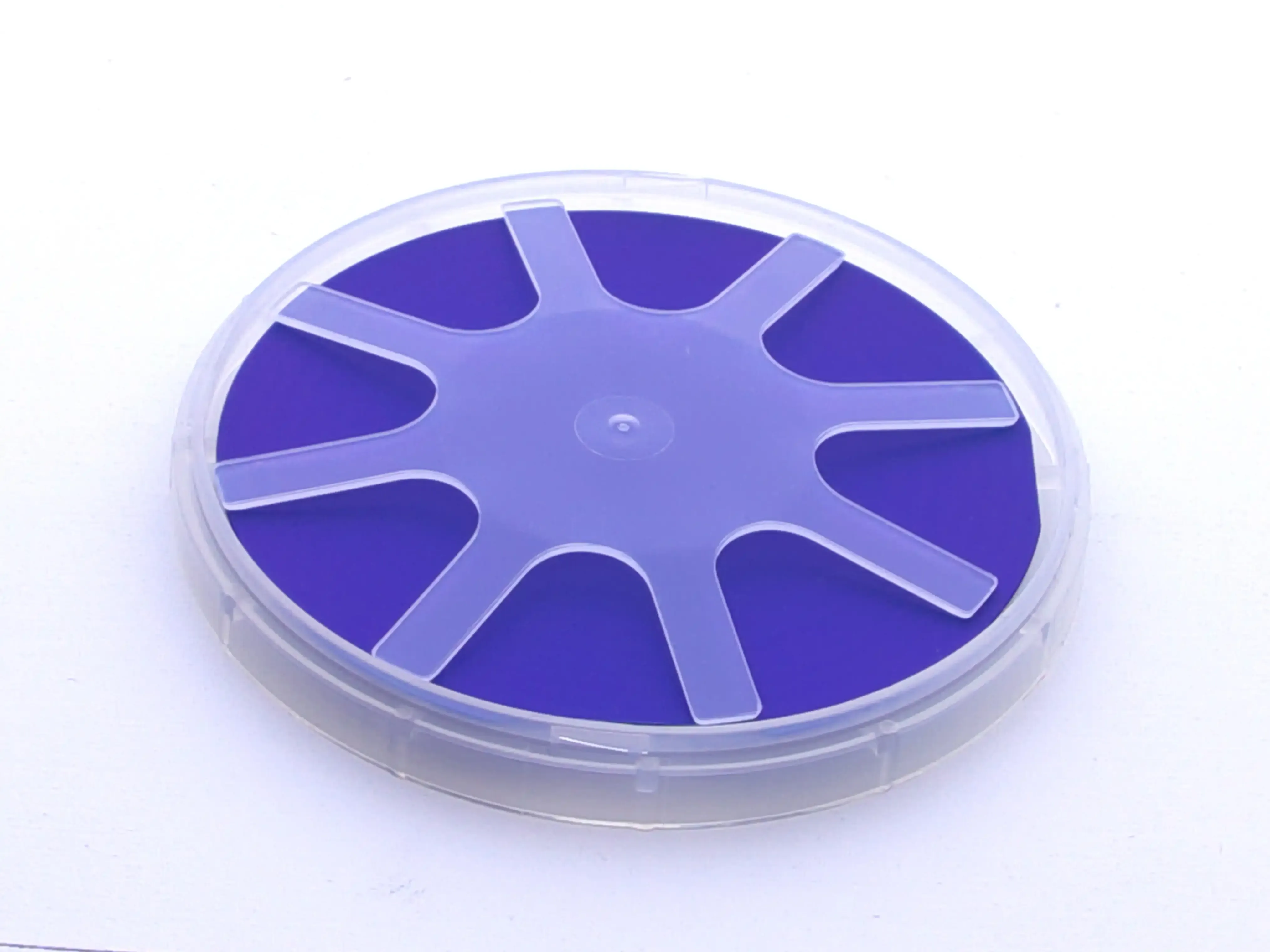
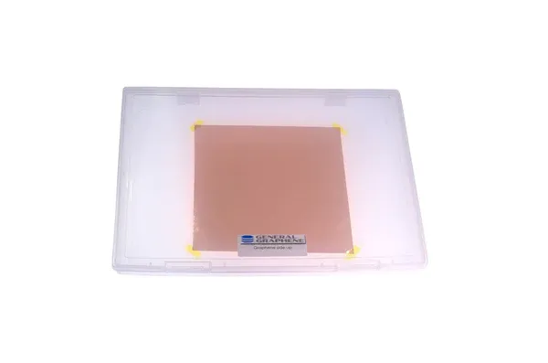
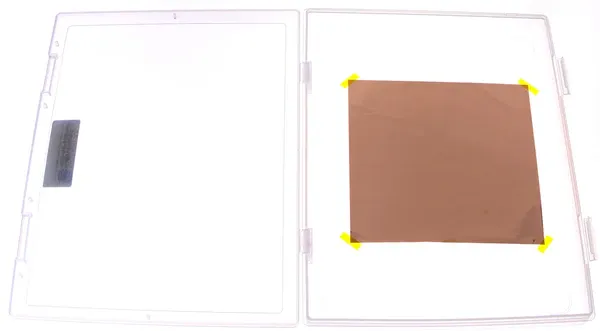
Monolayer CVD graphene on a 300 nm SiO2/Si wafer is a ready-to-use platform for graphene device fabrication, characterization and research. A single atomic layer of graphene is grown by chemical vapor deposition on copper foil and then moved onto a standard 4 inch silicon wafer with a thermal oxide layer through a wet transfer process, so the film arrives on the substrate most labs already use for field-effect transistors and sensors.
Graphene combines high electrical conductivity, high carrier mobility and high optical transparency in a two-dimensional film. On an oxidized silicon wafer the graphene is easy to locate by optical contrast and can be patterned, contacted and gated directly, which makes it well suited to graphene field-effect transistors (GFETs), electrochemical and biosensing devices, optical and optoelectronic studies, and electrode or interface research.
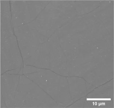
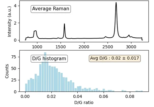
Film quality is verified by Raman spectroscopy, SEM and optical microscopy, covering monolayer quality, defect level and graphene coverage on the wafer. The single-side polished wafer uses standard SEMI flats, which makes alignment straightforward in cleanroom workflows.
Substrate/Film type
Planar film
Coating
Graphene
Growth substrate
Predominantly Cu(111)
Cu Catalyst Thickness (µm)
20
Average Crystal Size (catalyst)
cm-scale
Transfer Method
Wet transfer
Film Thickness
3.45 Åm
Transparency
~97.7%
Average Graphene Grain Size (µm)
~80
Multilayer Coverage (%)
< 5%
Graphene Coverage on Wafer
> 90%
I2D/IG Average - after transfer
> 1.6
ID/IG Average - after transfer
< 0.05
2D peak FWHM (cm-1) - after transfer
~ 35
Dirac Point (mV)
220 ± 40
Sheet Resistance
600 ± 50 Ω/sq
Mobility (cm2/Vs)* (dep on transfer)
2400 ± 230
Wafer Type/Dopant
P-type (Boron)
Wafer Growth Method
CZ Prime
Wafer Orientation
<1-0-0>
Wafer Resistivity (Ω·cm)
< 0.005
Oxide Layer
Wet oxide on both sides, 3000 Å ± 5%
Wafer Finish
Single-side polished
Wafer Flats
2 SEMI
Growth Method
Chemical Vapor Deposition (CVD)
Quality Control
Raman, SEM, Optical
Substrate Thickness (um)
525 ± 25
Appearance
Transparent film
Size
100 mm (4 inch) wafer
Get pricing and product details from General Graphene.
0 global ratings
Verified Identity
Every review undergoes an email verification process to ensure it originates from a verified industry professional.
Verified Purchase
We manually validate "Verified Purchase" claims by cross-referencing with supplier records or identifying the equipment in peer-reviewed scientific publications.
Transparent Publishing
All verified reviews, whether positive or negative, are published without bias as long as they comply with our community guidelines.
No reviews yet. Be the first to share your thoughts!
Share your experience with this product.
Help the scientific community by sharing research papers that utilize this equipment.
Contact us to add your research.
Price: from 90.00 USD
Price: from 100.00 USD